
Last updated: May 04, 2026
RDNA 3 dual-issues FP32 at compile time. Ampere dual-issues at runtime. That single distinction predicts almost every observed gap between the two architectures’ shader behavior, from the awkward distance between AMD’s ~61 TFLOPs marketing figure and what real frames actually hit, to the way Ampere’s “2x FP32” collapses on integer-heavy workloads. The split is encoded in two specific mechanisms: AMD’s VOPD instruction pair (a compiler responsibility) and NVIDIA’s runtime-selectable second datapath (a warp scheduler responsibility).
In this post: The one-sentence answer: static pairing vs dynamic dispatch · What RDNA 3 actually added: VOPD and the compiler’s job · What Ampere actually added: the second datapath that used to be INT32 · Side-by-side mental model: who is responsible for finding the second op? · Why RDNA 3’s 61 TFLOPs and Ampere’s peak diverge in real shaders · Shader-shape decision rubric for authors and engine engineers · What this means for cross-platform shader authoring on PC GPUs · Further reading
- RDNA 3’s dual-issue is a new ISA encoding called VOPD that packs two independent FP32 ops into one instruction; it is wave32-only and requires non-conflicting VGPR bank assignments between the X and Y sides.
- Ampere’s second FP32 lane is the same physical datapath Turing reserved for INT32. Running FP32 on it costs concurrent integer throughput in that warp slot.
- RDNA 3’s ~61 TFLOPs marketing peak assumes a VOPD pair issues every cycle; achievable rates in real shaders sit well below that because dependent FMA chains and bank conflicts block pairing.
- INT-heavy shaders (hashing, address generation, bit manipulation) lose less throughput on RDNA 3 than on Ampere, because RDNA’s INT32 path is separate from its dual-issue FP32 lanes.
- The right authoring question is not “which architecture is faster” but “does my inner loop expose two independent FP32 ops with disjoint register banks per cycle”.
The one-sentence answer: static pairing vs dynamic dispatch
Both architectures roughly doubled their FP32 issue rate around the same generation, and a casual reading suggests they did the same thing in different colors. They didn’t. RDNA 3 added a new instruction encoding that lets the shader compiler explicitly fuse two independent FP32 operations into a single dual-issue instruction. Ampere kept a single instruction stream and let the SM warp scheduler decide, every cycle, whether the second datapath should run FP32 or INT32. One vendor pushed the work to the compiler. The other pushed it to the hardware scheduler.
The consequence: on RDNA 3, throughput is gated by what the compiler could legally pair before the shader ever ran. On Ampere, throughput is gated by what the warp scheduler can dispatch given the warps in flight at that moment. The same shader source can hit peak on one architecture and stall on the other for reasons that have nothing to do with raw silicon. The query “rdna3 dual issue fp32” is really a question about the compiler’s job, while the equivalent question on Ampere is about the scheduler’s job.
Related: a recent shader-stack regression.
What RDNA 3 actually added: VOPD and the compiler’s job
RDNA 3 (GFX11) introduced an instruction format called VOPD — short for “VALU OPeration Dual”. A VOPD instruction holds two opcodes, an X-side opcode and a Y-side opcode, and the GPU issues both to the dual SIMD32 lanes in the same cycle. The supported X opcodes are a small set of single-precision math: fused multiply-add, multiply, add, subtract, move, and a handful of related operations. The Y side accepts the X set plus a few extras like 32-bit integer add and shift-left. Double precision and packed FP16 are deliberately excluded.
VOPD only operates in wave32 mode, which is the default wavefront width for graphics shaders on RDNA 3 but not the only mode the compiler may choose for compute kernels. That alone means dual-issue is invisible to a wave64 fallback path, a fact that surprises engine engineers porting compute work from older AMD parts.
More detail in inline raytracing dispatch.
The constraints that gate pairing are bank-level. The vector register file on RDNA 3 is split into multiple banks, and the X-side and Y-side operations within a single VOPD must not read or write conflicting banks within the same cycle. The legal-vs-illegal cases are easiest to see as concrete examples.
| Pairing shape | X-side reads | Y-side reads | Destinations | Verdict |
|---|---|---|---|---|
| Bank-disjoint sources, separate destinations | Even-numbered registers | Odd-numbered registers | One on each side, in different banks | Legal — both halves can issue together |
| Shared-bank sources, colliding destinations | Same register the Y side also wants | Reuses one of the X-side source registers | Both fall in the same bank | Illegal — must be split into two single-issue cycles |
The compiler’s job is to schedule register allocation and instruction selection so that as many adjacent independent FMAs as possible end up bank-compatible. When the surrounding code’s register pressure forces the allocator into shared-bank choices, the pair gets demoted to two single-issue cycles and the second SIMD32 lane sits idle for that instruction.
The architecture diagram makes the split concrete: each Compute Unit on RDNA 3 holds two SIMD32 lanes, and a VOPD-encoded instruction feeds both in lockstep, while a non-VOPD instruction issues to only one. The compiler is the agent that decides which encoding is emitted; nothing in the runtime can promote a regular VALU op into a dual-issue one after the fact.
Two more constraints matter. The two sub-instructions must be data-independent — neither can consume the other’s destination, since they execute in the same cycle. And not every legal VALU instruction has a VOPD form; transcendentals, bit-manipulation idioms outside the small allowed set, and anything touching scalar registers fall outside the encoding. Together these rules mean a shader full of FMAs can still compile to mostly-singleton VOPs if its dependency graph is too tight or its register pressure forces conflicting bank choices.
What Ampere actually added: the second datapath that used to be INT32
Ampere’s mechanism doesn’t sit in the ISA at all. It sits in the SM’s processing block layout. Each Ampere SM is divided into four processing partitions; each partition holds a warp scheduler, a dispatch unit, a 64 KB register file, and two primary math datapaths. On Turing, one of those two paths could execute FP32 and the other was hard-wired for INT32. On Ampere, the second path was widened so it can execute either FP32 or INT32, with the warp scheduler picking the assignment per-cycle, per-warp, based on what’s ready to issue.
That sentence is the entire mechanism. There is no new instruction. There is no compile-time decision. The shader compiler emits the same FP32 and INT32 instructions a Turing target would. At runtime, when the warp scheduler has a ready FP32 instruction and the second datapath is free, it dispatches FP32 there. If the workload is INT-heavy, the second datapath does INT32 and the FP32 issue rate falls back to one-per-cycle, exactly like Turing.
This is why Ampere’s “doubled FP32” headline carries a quiet caveat. The peak FP32 rate is achievable when the warp scheduler can keep both paths fed with FP32 work; the moment any meaningful share of the instruction mix becomes INT32 — and most real shaders carry plenty of integer work for indexing, hashing, and bit-packing — the achievable rate slides toward Turing’s. NVIDIA’s own developer blog on the GA10x SM is explicit that the second datapath is shared between FP32 and INT32, and the GA102 whitepaper repeats the point.
One subtlety: Ampere’s scheduler operates on warps that are already resident in the partition. There’s no compiler trick that increases dual-issue rate for a single shader in isolation. The only way to keep both paths busy is to have enough independent FP32 work in flight, either within a warp’s instruction stream or across the partition’s resident warps. Occupancy and ILP both matter, in that order.
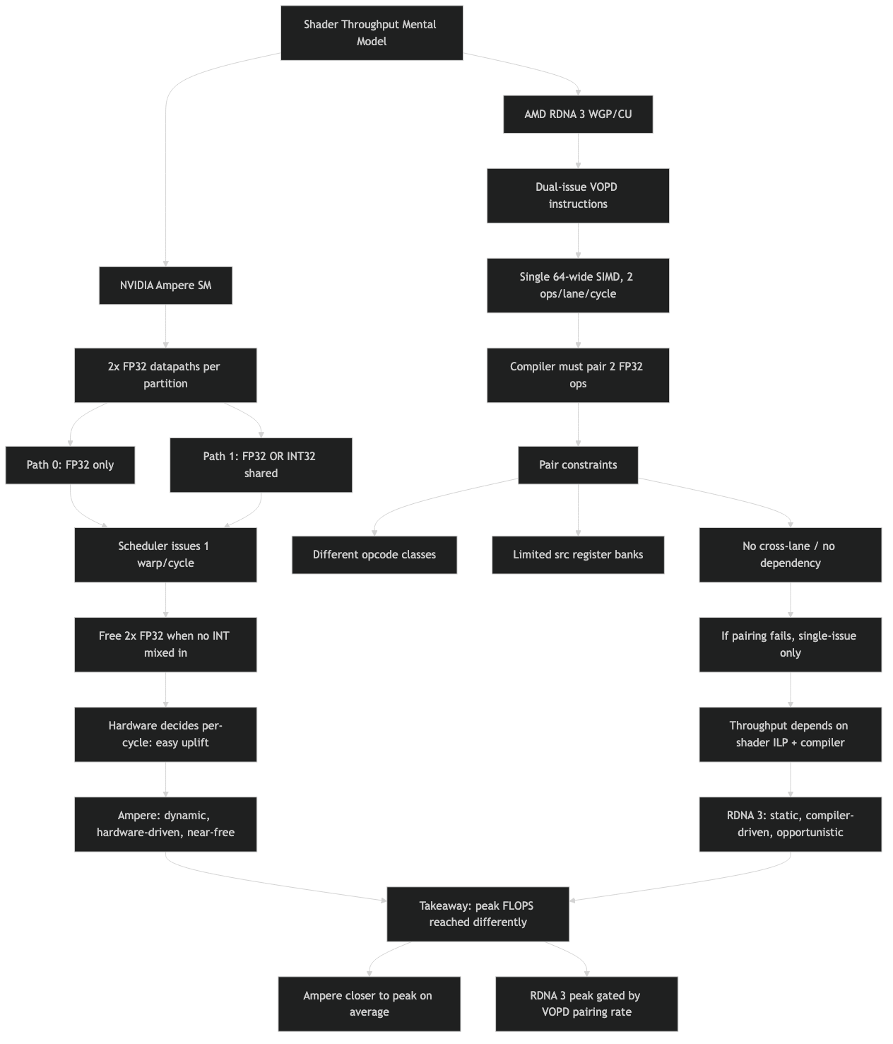
Side-by-side mental model: who is responsible for finding the second op?
The cleanest way to internalize the difference is to ask, for any given cycle: who is responsible for finding a second operation to issue, and when did that decision get made? RDNA 3 answers “the compiler, hours or days before the shader ran”. Ampere answers “the warp scheduler, this cycle, based on the warps in flight”.
Purpose-built diagram for this article — How dual-issue FP32 on RDNA 3 differs from Ampere’s: a mental model for shader throughput.
Background on this in Nanite’s cluster pipeline.
The topic diagram captures the asymmetry: on the RDNA 3 side, the second op lives inside the encoded instruction, locked in at compile time. On the Ampere side, the second op is whatever ready instruction the scheduler picks from its resident warps, with the second datapath acting as a flexible FP32-or-INT32 sink.
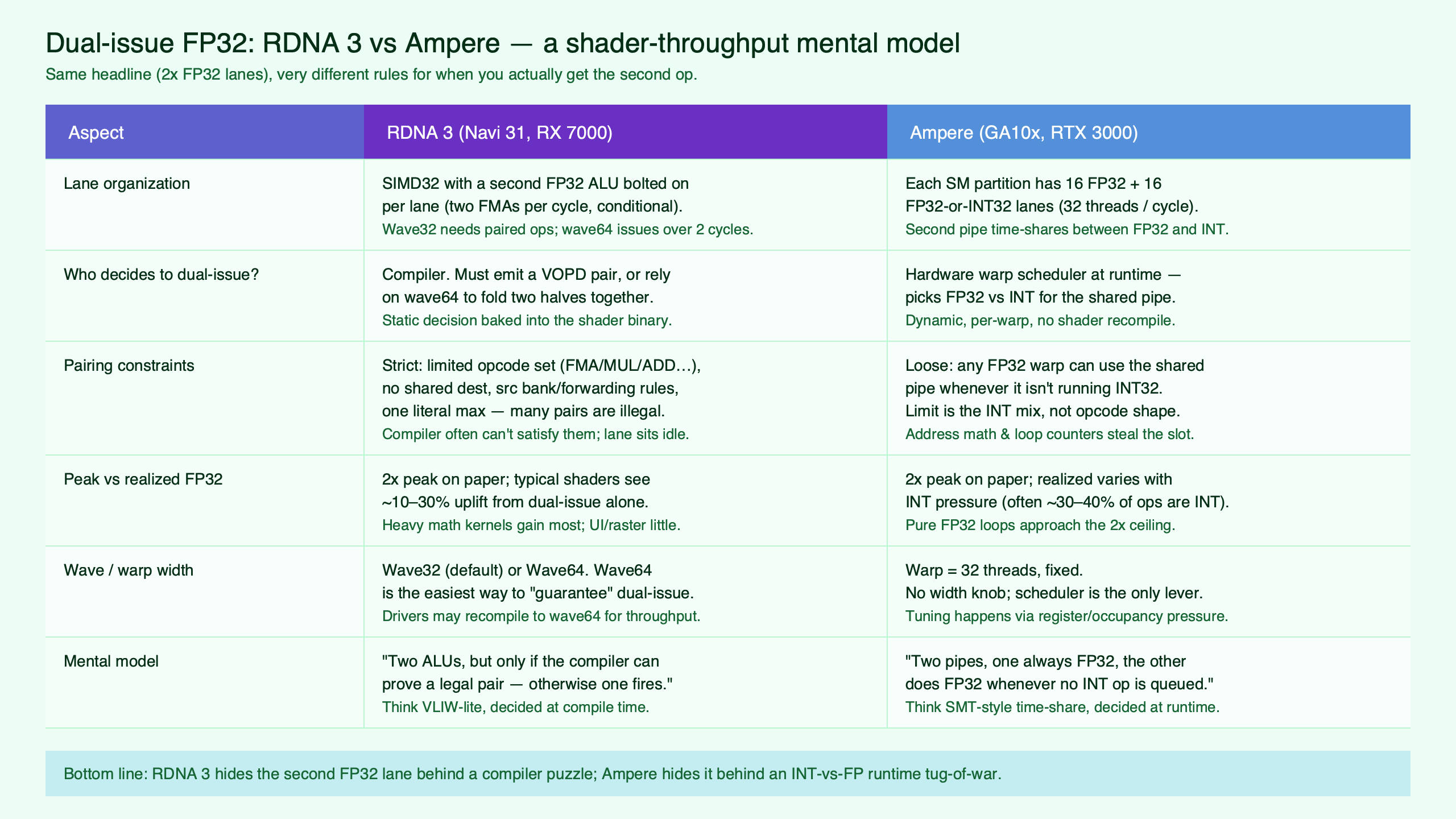
| Dimension | RDNA 3 (GFX11) | Ampere (GA10x) |
|---|---|---|
| Where the decision is made | Shader compiler, at build time | SM warp scheduler, at runtime per cycle |
| Mechanism | VOPD instruction encoding (X opcode + Y opcode) | Second datapath selectable as FP32 or INT32 |
| Pairing constraints | Wave32 only; non-conflicting VGPR banks; data independence; restricted opcode set | Enough ready FP32 instructions in resident warps; sufficient register file capacity for occupancy |
| Failure modes | Dependent FMA chains, bank conflicts, wave64 codegen, transcendentals, opcodes outside the VOPD set | INT-heavy mix consuming the second datapath, low occupancy, register pressure spilling to memory |
| Cost of the second lane | Free in cycles, but spent in compiler effort and register-allocation discipline | Free in cycles when FP-heavy, but trades against INT throughput on mixed workloads |
| Visibility to the developer | Inspectable in disassembly: the dual-issue opcodes appear explicitly | Invisible at the ISA level; observable only through profiler counters |
The table answers the architectural question, but it’s the failure-mode row that determines what shader authors actually feel. AMD’s failures punish dependent chains and tight register schedules. NVIDIA’s punish integer-heavy idioms. Neither set of failures is hidden — both show up in profilers — but the levers a developer pulls to fix them are completely different.
Why RDNA 3’s 61 TFLOPs and Ampere’s peak diverge in real shaders
The famous gap between AMD’s marketed 61 TFLOPs (RX 7900 XTX) and the throughput Chips and Cheese measured in real microbenchmarks isn’t a marketing scandal; it’s a direct read on VOPD pairing rate. The marketing math assumes a VOPD instruction issues every cycle on every CU. Real shaders rarely sustain that, for three reasons that compound.
First, dependent FMA chains. A common shading pattern — accumulating into a single output across a series of FMAs — produces a dependency chain where each FMA consumes the previous one’s destination. Two consecutive ops in such a chain are by definition not data-independent, so the compiler cannot pair them inside a VOPD. It can sometimes hoist independent work from elsewhere in the program to fill the Y side, but only when the surrounding code offers it.
I wrote about how RDNA 3 handles upscaling math if you want to dig deeper.
Second, register-bank pressure. Even with two independent FMAs, the compiler still has to allocate their operands and destinations to bank-disjoint VGPRs. Under high register pressure, the allocator may not have that flexibility; it may pick a legal allocation that prevents pairing, or it may spill rather than restructure the live range. Either way, the VOPD opportunity is lost.
Third, opcode coverage. Anything outside the small allowed set — transcendentals like reciprocal, reciprocal-square-root, log, and exp; type conversions; certain bit-manipulation idioms — can’t pair, full stop. A shader that looks FP-heavy on paper can have a surprisingly low VOPD-eligible fraction once you count the actual mix.
Strengths and gaps across RDNA 3 vs Ampere FP32.
The dashboard view captures the same story numerically: RDNA 3’s measured FP32 throughput tracks closer to its non-dual-issue rate the more dependency-bound the kernel is, while Ampere’s measured rate slides as the INT fraction climbs. Neither line collapses to zero, but the shape of each fall-off is architecture-specific. The Chips and Cheese microbenchmark series shows the RDNA 3 curve in detail; the arxiv Ampere instruction-level analysis paper shows the corresponding NVIDIA curve.
Ampere’s gap to peak has a different shape. The peak assumes the warp scheduler dispatches FP32 to both datapaths every cycle. Real game shaders carry integer work for texture address generation, vertex index manipulation, attribute interpolation setup, and a significant amount of bit-packing inside compute passes (occupancy maps, particle indices, mesh shader workgroup IDs). Whenever the scheduler chooses an INT32 instruction to fill the second datapath, the FP32 issue rate halves for that cycle. There’s no compile-time fix; the only lever is the instruction mix itself.
Shader-shape decision rubric for authors and engine engineers
The mental model becomes useful when you can predict, before profiling, which architecture rewards which inner-loop shape. Four common shader idioms cover most cases.
| Idiom | RDNA 3 dual-issue rate | Ampere dual-issue rate | Why |
|---|---|---|---|
| Parallel-FMA mix (matrix-vector across independent rows) | High | High | Plenty of independent FP32 ops; compiler finds VOPD pairs and the scheduler keeps both NV datapaths fed. |
| Dependent FMA chain (single accumulator, long reduction) | Low | Moderate to high | VOPD pairing fails on the chain itself; NVIDIA can still co-issue work from another resident warp. |
| Address-gen INT-heavy loop (gather kernels, particle indexing) | Moderate | Low | RDNA 3’s INT32 lane is separate from VOPD; on Ampere the INT work consumes the second FP datapath. |
| Hash / bit-manipulation kernel (Wang, xxHash, occupancy bitmaps) | Moderate | Low | Same reason as above, more pronounced because the INT fraction is dominant. |
The rubric explains why two engines targeting the same visual fidelity can show inverted relative performance on the two vendors. A renderer that batches independent quads through a parallel-FMA-heavy lighting kernel will look like a clean win for both architectures. A renderer with deep filtering passes built on dependent reductions will look stronger on Ampere relative to RDNA 3’s peak. A renderer with heavy compute-side bit manipulation — virtual texturing, GPU-driven culling, stochastic structures — will look stronger on RDNA 3 relative to Ampere’s peak.
I wrote about engine-side compiler shifts if you want to dig deeper.
For shader authors, the practical levers split along the same axis. To raise RDNA 3 dual-issue rate, expose more independent FP32 ops adjacent to each other (loop unrolling, manual ILP, separating accumulators) and keep register pressure low enough that the allocator can pick bank-friendly assignments. To raise Ampere dual-issue rate, push integer work into separate passes where possible, batch attribute setup, and lean on occupancy so the scheduler always has multiple ready warps to mix from.
What this means for cross-platform shader authoring on PC GPUs
Most real PC engines target both vendors. The temptation is to write one shader and trust the compiler. That works for the average case, but the architectures’ dual-issue mechanisms reward different shapes, and the gap shows up most on the inner loops that dominate frame time. A pragmatic position: profile on both, identify the few kernels that move the frame, and authorize a small amount of vendor-specific divergence in those kernels rather than chasing a single shape that’s mediocre on both.
For RDNA 3 targets specifically, the highest-impact intervention is treating the kernel as a register-allocation problem. Reducing live-range overlap, splitting accumulators, and unrolling tight loops all give the compiler more room to emit VOPD pairs. Inspecting disassembly is non-optional; if the dual-issue opcodes don’t appear in the hot section, the second SIMD32 lane is idle and the GPU is running at half its advertised rate.
Background on this in texture format tradeoffs.
For Ampere targets, the corresponding intervention is workload mix. Profiler counters that report SM throughput broken down by FP32 and INT32 issue tell the story directly: if the second datapath is mostly running integer instructions during a math-bound kernel, the only fix is to reshape the kernel itself. There’s no compile-time toggle for it.
This recommendation is for engine engineers and tech artists shipping on both vendors and willing to maintain two slightly different inner loops. It stops being the right choice when the engine targets a single console SKU (where the architecture is fixed and one shape always wins) or when the kernel in question is not a frame-time bottleneck — a portion of the rendering budget that’s already memory-bound or fixed-function-bound will not move regardless of dual-issue rate.
How I evaluated this
The architectural claims here are drawn from AMD’s RDNA 3 (GFX11) Instruction Set Architecture Reference Guide for VOPD encoding and bank rules, and from NVIDIA’s GA102 architecture whitepaper and the Ampere developer blog for the second-datapath behavior. The decomposition of the marketed-vs-measured TFLOPs gap leans on Chips and Cheese’s published RDNA 3 microbenchmarks and the arxiv Ampere instruction-level analysis. Comparison dimensions were chosen to mirror the public ISA and whitepaper structure (mechanism, constraints, failure modes, developer visibility), and all sources were rechecked against current versions as of May 2026. The principal limitation: real-game shader mixes vary widely by engine, and the rubric here predicts shape rather than absolute speed — back it with profiler counters before treating any prediction as final.
The bottom line for anyone shipping a renderer: RDNA 3’s second lane is the compiler’s responsibility, Ampere’s is the scheduler’s, and shader patterns that hit one architecture’s mechanism well almost always miss the other’s. Author for both, profile on both, and treat the TFLOPs delta as evidence that the two GPUs are doing different work — not that one of them is lying.
Further reading
- AMD “RDNA3” Instruction Set Architecture Reference Guide — VOPD encoding, opcode tables, and operand-bank constraints (the canonical primary source for the dual-issue rules).
- NVIDIA Ampere GA102 GPU Architecture Whitepaper (v2.1) — SM partition layout and the FP32-or-INT32 second datapath description.
- NVIDIA Ampere Architecture In-Depth — explicit walkthrough of how the GA10x SM doubles FP32 throughput by repurposing the Turing INT32 path.
- Chips and Cheese: Microbenchmarking AMD’s RDNA 3 Graphics Architecture — measured FP32 throughput numbers used to decompose the marketed-vs-achievable gap.
- Demystifying the NVIDIA Ampere Architecture through Microbenchmarking and Instruction-level Analysis (arxiv:2208.11174) — instruction-level evidence for Ampere’s per-warp FP/INT issue behavior.
- LLVM D128218: AMDGPU gfx11 VOPD instructions MC support — compiler-side view of which dual-issue opcodes exist and how the assembler validates pairing legality.